PCB testing sits at the point where recycling meets real chemistry. If you’ve ever wondered why two “similar” circuit boards can be valued very differently, the answer is usually in how they’re inspected, sampled, and analysed. This guide walks through the common lab and yard methods used to grade and test printed circuit boards (PCBs) and mixed electronics streams - starting with simple visual grading and ending with ICP-OES, one of the go-to tools for measuring metals after digestion. The goal is to make the process feel technical but still easy to follow, so you know what’s happening behind the scenes when boards are sorted, sampled, and valued.
In e waste recycling, PCBs are a high-information material. They can contain base metals (like copper), precious metals (like gold and silver), and a wide range of other elements depending on the device and era. However, a board’s value and processing route depend on what’s actually present, not what we hope is present.
That’s why testing exists at all. It helps answer practical questions such as:
It also supports trust. When a recycler can show a clear chain from intake, to grading, to sampling, to lab results, the valuation becomes easier to explain and easier to repeat.
The diagram below shows how a batch of boards moves from intake to a defensible valuation. Each step builds on the last, and the quality of the final result depends on getting the earlier stages right.
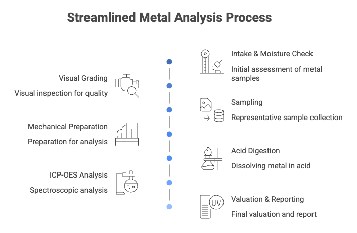
Grading is a quick classification based on visible features. Testing is a measurement process that estimates or quantifies the metals and other elements in a sample.
Grading often happens first because it’s fast and cheap. Testing comes in when the load is large, mixed, disputed, or valuable enough that a measured result is worth the extra time.
Visual grading is the front line. A trained sorter can spot patterns in seconds: connector density, chip count, board thickness, and the presence of gold-plated edges. While it’s not a chemical analysis, it’s surprisingly effective when the stream is consistent.
Sorters typically look at the parts that tend to correlate with metal content:
Visual grading can drift when a stream changes. A batch of “similar-looking” boards may come from different manufacturers, years, or device types. Also, modern miniaturisation can fool the eye: smaller boards can still be metal-rich, while large boards can be surprisingly low in target metals.
That’s where testing adds value. It checks the assumptions that visual grading makes.
Before a sample ever hits a lab bench, a few practical intake checks can protect the accuracy of later testing. These checks also reduce delays because the lab can work with a cleaner, more consistent sample.
Wet loads cause headaches. Moisture changes weight, encourages corrosion, and can complicate safe handling when batteries are present. If a batch has been stored outdoors, a recycler may need to dry or stabilise it before sampling. That way, the result reflects the boards, not the weather.
Heatsinks, steel frames, cables, and housings can swamp the sample with non-target material. Even if those parts have their own recycling route, leaving them attached can dilute the PCB fraction and distort any “per tonne” estimates derived from lab numbers.
If you’re sending electronics as part of a business clear-out, it’s worth reading practical prep guidance like e waste preparation steps before collection. Small prep choices often lead to smoother sorting and more consistent grading downstream.
A representative sample is one that reflects the average makeup of the whole batch. That sounds simple, but it’s the part most likely to cause disputes if done casually.
For mixed PCBs, sampling usually means combining many small increments from across the load, rather than grabbing “the best-looking boards” from the top.
Documentation matters here. Photos, container counts, batch weights, and sample IDs help keep the story straight if someone asks, “Where did this number come from?” three weeks later.
Labs and large recyclers often reduce the PCB material to smaller pieces before chemical work. The reason is simple: metals and components are not evenly distributed across a board. If you test a single corner, you might hit a connector-rich area and overestimate.
Size reduction and mixing aim to make the material more uniform so that a small test portion behaves like the larger batch.
Even after shredding, PCBs contain a mix of metals, glass fibre, resins, and solder. Some fractions grind differently. Some metals appear as fine particles while others stay in larger fragments. Good labs and processors account for this by using consistent preparation steps and by avoiding shortcuts that concentrate heavier particles in one spot.
ICP-OES (Inductively Coupled Plasma Optical Emission Spectrometry) is a lab method used to measure elements by turning a prepared sample into a liquid and then reading the light emitted by atoms in a plasma. In practical terms, it can quantify multiple metals in one run, which makes it popular for complex recycling samples.
Scientific studies on PCB assays commonly use acid digestion followed by ICP-OES to quantify metals in scrap boards, including base and precious metals, because the technique can handle multi-element analysis efficiently. See an example study using ICP-OES on scrap mobile phone PCBs after acid digestion.
ICP-OES generally needs a liquid sample. PCBs are solid and complex, so labs use digestion to dissolve the target elements into solution. The exact acids and steps depend on what the lab needs to measure and how the method is validated.
A good digestion step aims for consistent recovery. That means the metals of interest move into the liquid phase reliably, so the instrument reads them accurately. If digestion is incomplete, the test can under-report certain elements because some of the sample never became measurable.
PCBs aren’t a single material. They include copper tracks, solder alloys, plated contacts, ceramic components, and resin-glass composites. Some parts dissolve readily, while others resist. Labs choose digestion methods that match the target analytes and the matrix, then confirm performance with standards and controls.
After digestion, the lab runs the sample through the ICP-OES. The output is typically element concentrations (often as mass per mass in the solution, then back-calculated to the original solid sample). For valuation and processing decisions, what matters is not just a single number, but how consistent the numbers are across repeats and across sub-samples.
Research into PCB characterisation also highlights how sample preparation and exploratory chemical analysis shape the quality of ICP-OES results. This Detritus Journal article discusses PCB chemical analysis using ICP-OES and related preparation considerations.
Most operations use both. Visual grading is the fast filter. ICP-OES is the proof point when you need measured chemistry.
| Method | What it’s good for | Limitations | When it’s most useful |
|---|---|---|---|
| Visual grading | Speedy sorting, separating obvious high/low grade boards | Relies on experience and assumptions; struggles with mixed or modern miniaturised boards | High-volume intake, consistent streams, first-pass classification |
| Weight-based checks (including attachment removal) | Spotting dilution from housings, heatsinks, and mixed materials | Does not identify metals; only indicates composition changes | When loads arrive with attachments or uncertain preparation |
| Lab digestion + ICP-OES | Multi-element measurement for more defensible valuation and QA | Needs proper sampling and prep; results depend on method validity | High-value lots, disputed grades, mixed streams, audit-ready reporting |
Electronics recycling rarely arrives as “perfect PCBs only”. Real loads can include cables, power supplies, metal housings, and sometimes unexpected items. As a result, good operators think in streams: boards, ferrous, non-ferrous, and special categories.
If your incoming material includes separate metal fractions (for example aluminium heatsinks or copper-heavy wiring), it can help to route those parts through a dedicated metal stream. Blancomet covers this kind of separation with services that sit alongside electronics processing, such as scrap metal recycling, where clean separation supports clearer weights and cleaner outputs.
Searches like e waste recycling near me or e waste near me usually mean the same thing: you want a legitimate handler close enough to make logistics simple, but competent enough to manage data risk and material value.
Distance matters, but it shouldn’t be the only filter. For PCB-heavy loads, ask whether the recycler can explain their grading categories, how they sample mixed boards, and what testing they use when results need to be defensible.
Ask for clarity, not jargon. A trustworthy testing and valuation workflow should be easy to describe in steps.
If you’re building a wider programme (devices, data, collections, and reporting), this topic sits inside a bigger operational picture. It’s also covered in more depth in E-waste Recycling & IT Asset Disposal, especially where PCB value streams connect to compliant handling and documentation.
PCB testing doesn’t only serve recycling. Understanding what’s inside a board also helps inform decisions earlier in the product lifecycle — including whether a device should be repaired, refurbished, or recycled in the first place.
When boards are tested and found to contain relatively low recoverable value, or when the device they came from is still functional, the economics can favour repair over shredding. In fact, the environmental and financial case for extending device life is often stronger than most people assume. Blancomet explores this idea in detail in their article on why fixing electronics is better than replacing them, which looks at how repair reduces demand for raw materials and keeps usable technology in circulation longer.
For recyclers and businesses alike, this creates a useful decision tree: grade the material, test where needed, and route each item to its highest-value outcome — whether that’s recovery, refurbishment, or reuse. Good testing data makes that routing decision more confident and less wasteful.
You don’t need a lab to make lab results better. Small handling choices can reduce ambiguity and make your stream easier to grade.
If you already know you have server boards, telecom backplanes, and low-grade appliance boards, separate them into distinct containers. Mixed loads force broad averaging, which usually helps nobody.
Steel cases, large aluminium heatsinks, and bulky plastics can dilute a board fraction. If removal is safe and sensible, do it. If not, tell the recycler what’s included so they can plan sorting time.
This protects people and helps with compliance. It also prevents a single risky item from slowing down the whole batch.
A simple note like “mostly office IT from a 2018-2022 refresh” can help set expectations and reduce mis-grading.
Different loads call for different routes. Sometimes you have board-rich material. Sometimes it’s mixed devices. Sometimes it’s mostly metal with a bit of electronics attached. Blancomet’s service pages can help you match the right pathway to the right material type:
PCB testing is a chain, not a single machine. Visual grading sets expectations, sampling protects fairness, preparation makes the material consistent, and ICP-OES provides measured chemistry that supports valuation and quality control. Good testing data also feeds smarter decisions upstream — helping businesses and recyclers determine whether a device is best routed to recovery, refurbishment, or reuse. If you’re sending boards or mixed electronics into a recycler, focusing on separation, safe preparation, and documentation usually pays back in fewer surprises. For organisations that need a clear route for devices, components, and board-bearing equipment, Blancomet’s recycling services provide practical pathways that connect collection and sorting to responsible downstream processing.
1. Is visual grading “good enough” for e waste?
It can be, especially for consistent streams where the same device types arrive repeatedly. Problems start when loads are mixed, modernised, or contaminated with attachments. In those cases, testing helps confirm what visual grading can only estimate.
2. What does ICP-OES actually measure in PCB testing?
ICP-OES measures elements in a prepared liquid sample, often after acid digestion of a shredded, homogenised PCB fraction. The result is typically a set of concentrations for multiple elements, which can then be used for comparisons and calculations.
3. Why do two batches of similar-looking boards test differently?
Small design differences change chemistry. Component mix, plating thickness, solder types, and board construction vary by manufacturer and year. Even within the same visual category, the metal distribution can shift enough to show up in lab numbers.
4. How can I improve the result if I’m searching e waste near me and want a fair assessment?
Separate obvious grades, keep boards dry, remove bulky non-board attachments if safe, and isolate batteries and storage media. Also share basic context about the source devices. Those steps make sampling more representative and grading more consistent.
5. Does scrap metal recycling overlap with e-waste handling?
Yes, in real collections it often overlaps. Many electronics contain valuable non-ferrous metals in frames, heatsinks, and wiring. Separating these fractions can reduce dilution of the PCB stream and make both routes clearer for sorting and processing.

5 Rosemount Park Drive
Rosemount Business Park, Ballycoolin Dublin, D11 FVH2, Ireland